A500ide, a simple non-autobooting IDE Hard disk interface for Amiga
500
Updates
Note: pcb print shows old www address in upper case, when lowercase letters were used in the link. current link is http://mkl211015.altervista.org/ide/a500ide.html
Future updates may appear here, as separate packages, i.e
for PCB design, software (driver and other), readme-docs etc..
Software, drivers.. LHA (9-dec-2005)
note: the ide.device in this archive is probably compiled to use the
base address $F20000, instead of $DA0000
AIDE
Zipped V1.11 PCB design
This "AIDE" PCB is a part of "a500ide". The board design is not necessarily
verified. Postscript files for Bottom copper layer, Top component placing
overlay and an *OPTIONAL* top copper layer. The optional top copper layer can
be substituted with wire links on the board and to the edge connector.
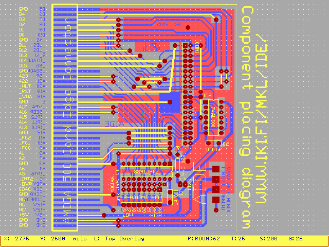
Screenshot from the PCB layout program in PNG and GIF formats. The
screenshot shows top copper layer in red, bottom copper layer in blue and
component placing in yellow. Also there are PNG and GIF for the
schematic.
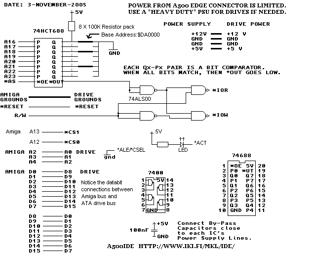
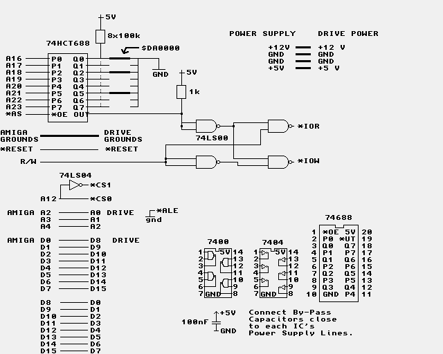
The following shows which address line goes to which pin on 74HCT688 in aide pcb.
You can choose any of the 8 bit-comparators on this chip for any address bit,
so it might it easier to assemble the interface on a "proto-board"
     ____ ____
*AS |1      20| +5V
A23 |2      19| *OUT (Goes low when address matches and *AS goes low)
S23 |3      18| S22  Comparator Q input "Sn" correspond to P input "An"
A21 |4      17| A22  Set all "Sn" same as "An" of the desired board address
S21 |5      16| S20  E.G.:
A19 |6      15| A20  Board address = hex $F2xxxx = binary 11110010
S19 |7      14| S18  so S23..S16 are "HHHHLLHL" or in other words
A17 |8      13| A18  DIP switch setting: off-off-off-off-on-on-off-on
S17 |9      12| S16  (or on-off-on-on-off-off-off-off to other direction)
GND |10     11| A16  (AIDE 1.11 has preset $DAxxxx by  cuttable PCB traces)
     ---------
                    TABLE   SIGNAL ASSIGNMENTS FOR ATA

 ======================================================================
      Signal        Connector              Connector      Signal
       Name          Contact   Conductor    Contact        Name
 ======================================================================
     RESET-             1        1 |  2        2         Ground
     DD7                3        3 |  4        4         DD8
     DD6                5        5 |  6        6         DD9
     DD5                7        7 |  8        8         DD10
     DD4                9        9 | 10       10         DD11
     DD3               11       11 | 12       12         DD12
     DD2               13       13 | 14       14         DD13
     DD1               15       15 | 16       16         DD14
     DD0               17       17 | 18       18         DD15
     Ground            19       19 | 20       20         (keypin)
     DMARQ             21       21 | 22       22         Ground
     DIOW-             23       23 | 24       24         Ground
     DIOR-             25       25 | 26       26         Ground
     IORDY             27       27 | 28       28         PSYNC:CSEL
     DMACK-            29       29 | 30       30         Ground
     INTRQ             31       31 | 32       32         IOCS16-
     DA1               33       33 | 34       34         PDIAG-
     DAO               35       35 | 36       36         DA2
     CS1FX-            37       37 | 38       38         CS3FX-
     DASP-             39       39 | 40       40         Ground
  *  +5V (Logic)       41       41 | 42       42         +5V (Motor)     *
  *  Ground (Return)   43       43 | 44       44         TYPE- (0=ATA)   *
         * Pins which are additional to those of the 40-pin cable.
 ======================================================================


2.5" drives have 44-pin cable
Some questionable things
move.l
I once noticed that data got corrupted when using 32-bit
move.l command to perform a double 16-bit data transfer
to and/or from the 16-bit IDE Task File data register.
So the driver/other software should use only the 16-bit move.w
68000 asserts /AS and R/W = low at the same moment
When the 68000 processor is doing a write cycle, it asserts
both /AS and R/W at the same processor state (the processor states are
states S0..S7).
This circuit expects that R/W = low already, when the 74HCT688 pulls
its output low (indicating address is correct and *AS is low.)
If unlucky, there would be a small glitch where *IOR goes low,
though only *IOW should have action.
On the other hand, the effect of *AS assertion travels a brief moment
through the 74HCT688 and one 74ALS00 gate before reaching
the 74ALS00 NAND gate that drives the *IOR line, but R/W goes directly
to that gate. But when the write cycle is about to end, 68000 first
deasserts *AS, and in a later state it drives R/W high, so
there does not seem to be a similar place for trouble there.
Possible fix: use *UDS instead of *AS? *UDS will go low in later state than R/W and *AS. It will shorten the *IOW pulse.
Reference:
http://www.freescale.com/files/32bit/doc/ref_manual/MC68000UM.pdf
Too short cycle for genuinely slow interface of an IDE drive
I think that the official specification draft specifies a
longer assertion for certain signals in PIO mode 0, THAN
this circuit produces. To overcome this theoretical(?) problem,
wait states could be generated by the XRDY signal towards the Amiga
mainboard.
Signal integrity
The interface should have buffers in order to keep signals clean and to
isolate the IDE cable/drive from A500's internal signal lines. 74LS245
buffers could be used, but there's no place for these in this PCB design.
Also it should be considered how to arrange control signals for the
buffers. Since line driver buffers cause large electrical switching noise when
many signals
switch at the same time, there should be ground
plane on the PCB, as well as decoupling capacitors for the buffers' supply
voltage.
The IDE cable should be short rather than very long. Unterminated electrically long wires reflect back the energy when signal reaches dead-end, when it goes back it makes unwanted voltages at the IDE connector and CPU points.
It is probably a good idea to use a good quality factory made cable.
It can be shortened with sharp scissors, leaving two connectors.
The modern 80-wire ATA-cables should be better, since they have extra grounds.
Previous versions
Version 1.5 (278174 bytes) "BETA"
release with a new PCB for two chip circuit and CDROM driver.
V1.5 fixed A BUG in the PCB V1.3 layout.
schematic diagram for v1.5
PCB design for v1.5
Features: Automatic drive indentification.
ide.device sources included
Old software supports one hard disk drive / interface, no ATAPI.
New software patches by Radovan Kobularcik support
two drives and ATAPI CD-ROMs.
iderkspr.zip is a
"preliminary" version of this software, with possibly non-critical bugs.
This is also included in the v1.5 a500ide.lha in a lha archive.
Tested on KS1.3 and 2.05. Tested drives:
CP3044, WD Tidbit60, Seagate ST3850 and some others.
With KS2.04+, there must not be a FileSystem = L:FastFileSystem line in
the mountlist entry because FastFileSystem is in KS-ROM.
OLD schematics (V1.2) in a GIF
Use 74ALS00 instead of 74LS00. The one kilo-ohm resistor is not needed at all.
Old version 1.2 (215303 bytes)
Contains a PCB for a circuit with PAL16L8 and 74..245 buffers.
I couldn't get it work well (timing problems?), so I removed it from V1.3.