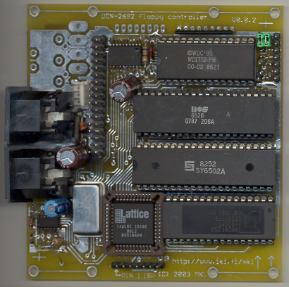
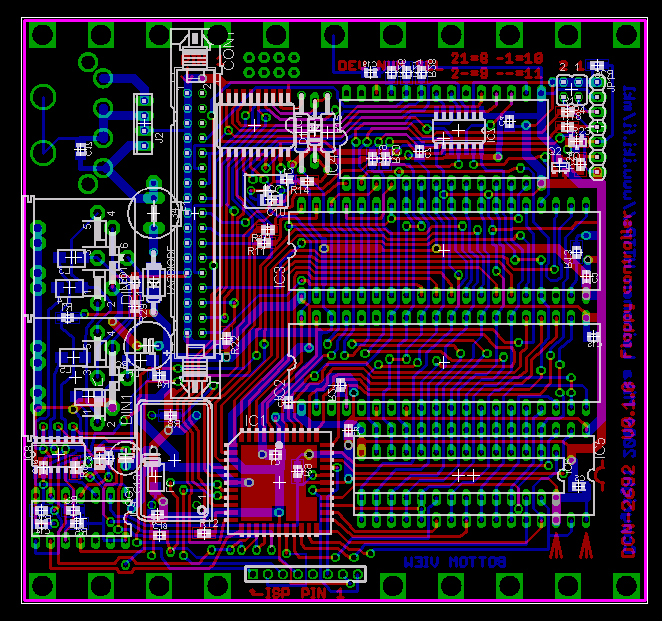
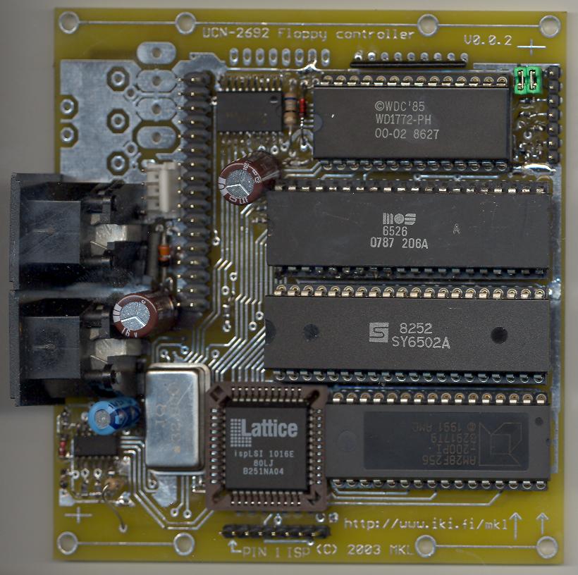
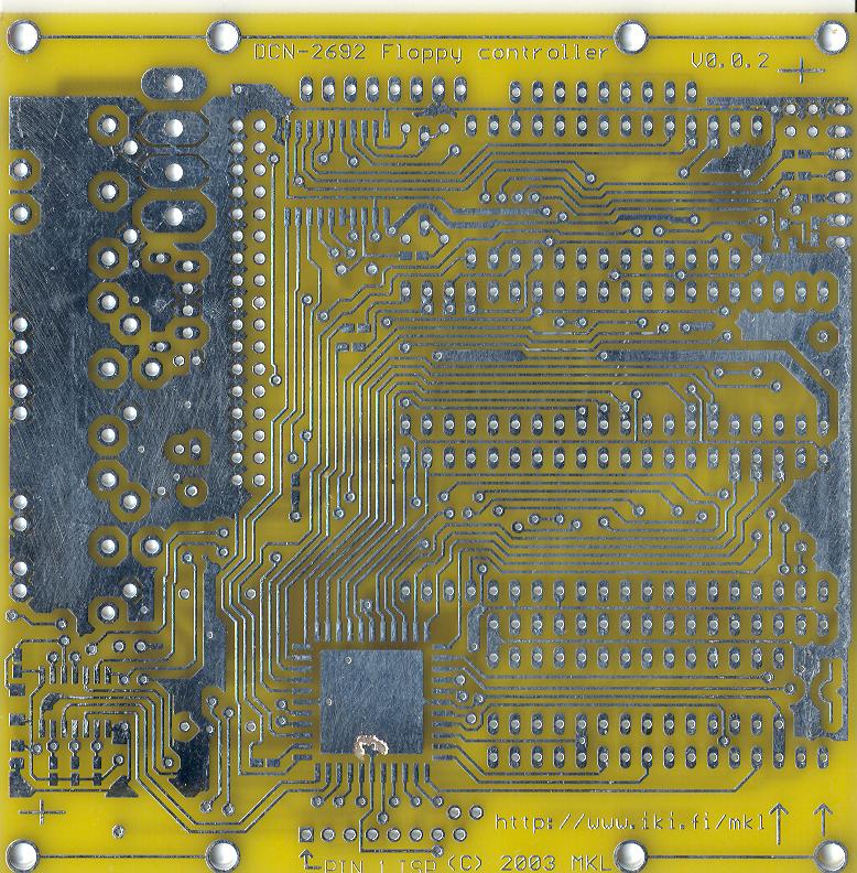
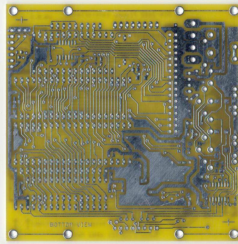
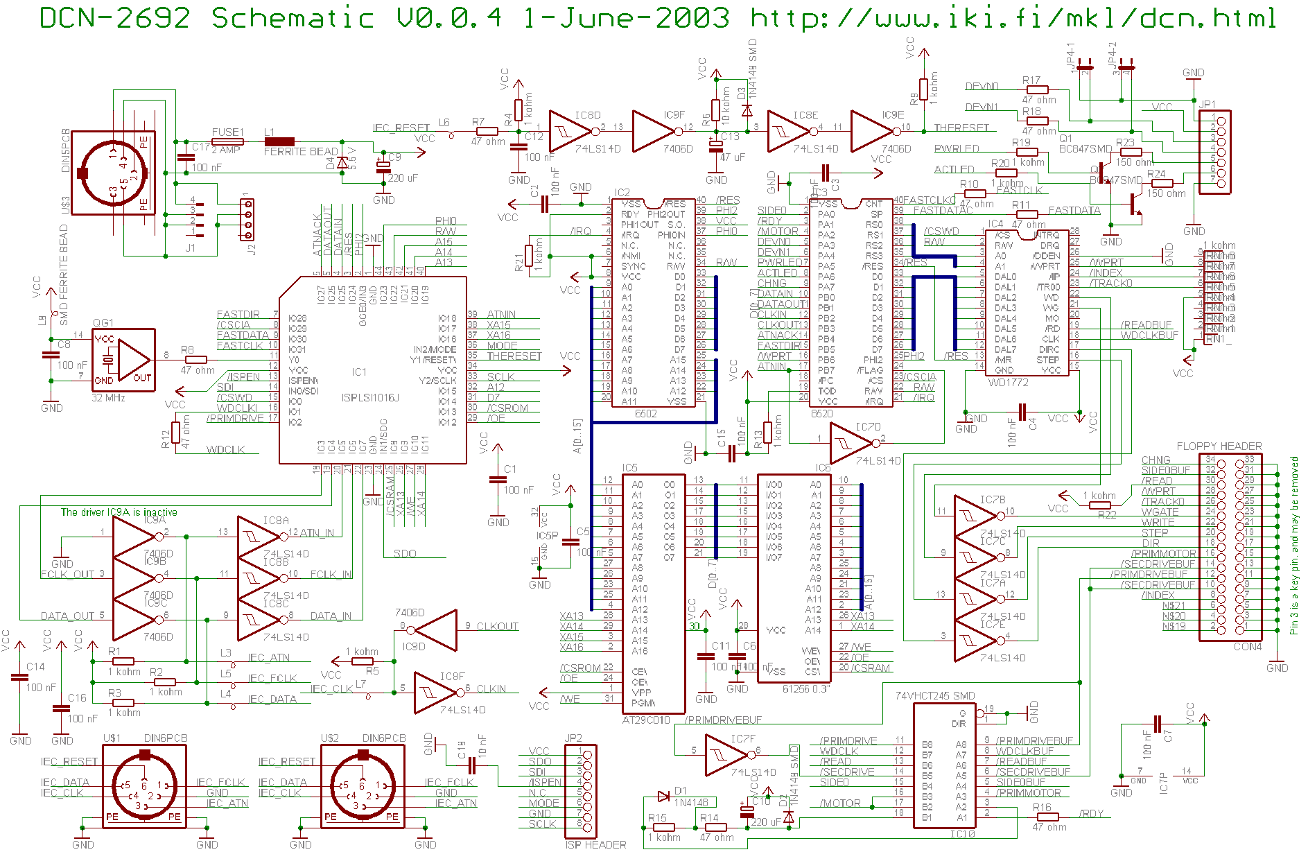
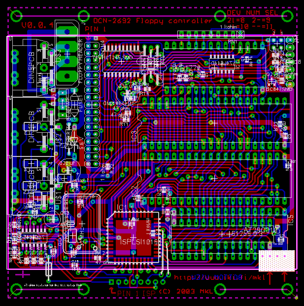
DCN-2692 floppy controller board
DCN-2692 "is" "suitable" to use with Commodores as a 1581 "clone"
PCB form factor differs from 1581, and intended to be used with "pc"-drive
This document was last modified 20-jan-2021 on 3-nov-2019 14-oct-2018 30-dec-2007
29-nov-2007 23-dec-2006
30-march 2006 26-march-2006 3-march-2006...

The above link is outside of this page you are currently viewing. There
will be links to related information, such as data of the ICs used.
Also follow the above link for other floppy controller projects & information.
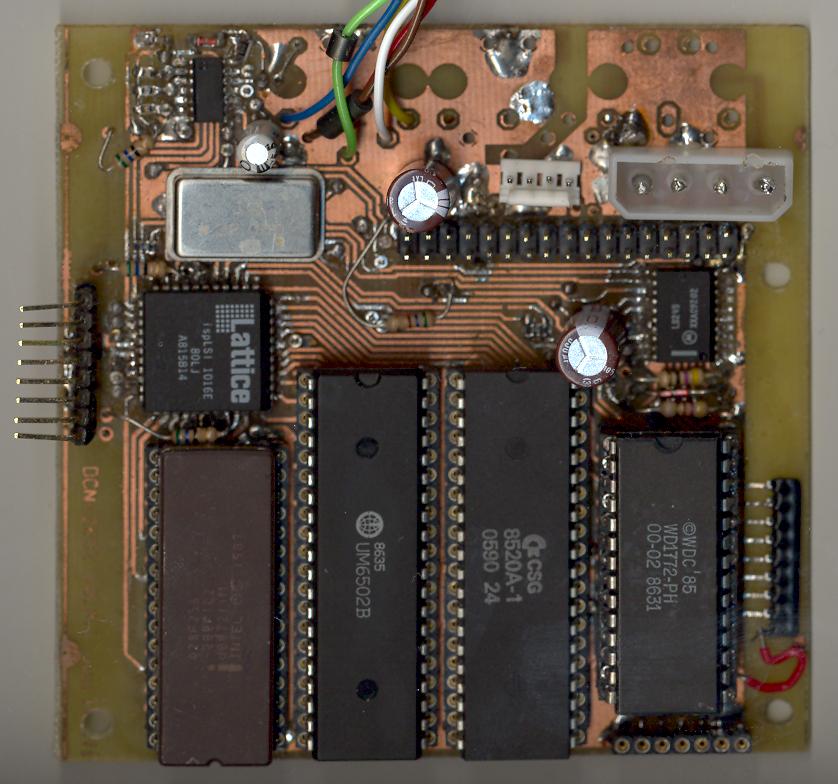
There are pictures of an early prototype of an 1581-clone.
If you plan to build one, please check if all necessary parts are
available (at a reasonable cost.) WD1772, for example, is rare.
Information about the board
The controller is intended to be used with a low cost
PC HD floppy drive unit.
Not all PC HD floppy drives are fully compatible. For example, the
JU-257A427P (I have rev. F) may fail. It does not respond fast enough to
the RW-head track-to-track stepping commands, and therefore the RW-head ends
up on a wrong track, which leads to data loss at worst. By changing
the code on the ROM on the board, the WD1772 Floppy Disk Controller could be
instructed to use the slowest setting for head-step. I have not tried this
modification in practise.
It is also rumoured, that the cheap drives of today are not of very high
quality, and not even really designed to be used with the obsolescent, hard to
find, Double Density floppies.
The floppy cable from the board to the drive is direct, without a
twist in the cable. Number 1 of of the cable and connector is near the
edge of the board. Odd numbered pins are grounds, except pin 3.
Number 3 of the connector is a key pin, and should be removed,
if the cable has a filled location, that does not accept a pin.
In a Commodore/Amiga DD-floppy mechanism, a few pins are different.
Some information on pinouts here
The activity LED on the drive unit will be normally
always lit, because the drive select signal from the board to the drive
unit will be normally always active, as in C-1581, where the drive
mechanism doesn't have a LED of it's own.
If a primary/secondary floppy drive selection signal will be implemented in the
programmable logic device in this design, the LED on the drive will indicate
which unit is selected at that time by the controller.
To use HD-floppies on a HD drive instead of DD-floppies, You can put
adhesive tape over the HD/DD-recognition hole. For some reason, without
that trick the HD-floppies do not seem to work. I do not know if
this could cause any reliability problems. Anyways, You shouldn't use
HD floppies on an DD only drive.
Jumpers and headers on the board
To select the device number for the Commodore serial bus, You can use
the jumpers at the top right hand corner of the board.
(see photo of board version 0.0.2 below.)
                            Jumper1 is the one which is closer to the board edge
Device number   Jumper2     Jumper1
      8         Closed      Closed
      9         Closed      Open
      10        Open        Closed
      11        Open        Open
Next to these jumpers, there is also a pin header,
which has the device select signals and outputs to connect two LEDs.
The LEDs can be connected between +5V and the output. Series resistors
for the LEDs are on the board. The Power LED in the CBM-1581 has two
functions: it is normally lit to indicate that power is on, and in case of
error or something special like that, the led blinks from dim to bright and
back. Since I wanted to make this board done finally allready, I omitted
the resistor that keeps the power led dimly lit. This resistor is added to
the board in version 0.1.0. The resistor can be added
to the circuit even if there is no place for it on the board. It is connected
between ground and the cathode of the power led, or pin 5 of the header.
The value of the resistor could be something between about 100 to 1000 ohms.
Pinouts for the header are, from the top right corner of the PCB:
1 GND
2 Vcc (+5V) (Anodes (+) of LEDs can be connected to this)
3 DEVN0 (device ID number select bit 0)
4 DEVN1 (device ID number select bit 1)
5 Power LED (Cathode -)
6 Activity LED (Cathode -)
7 GND
Powering the controller
The supply voltage should be 5 volts +-5% (4.75 - 5.25) at a max
current of about 1 ampere (could be much less actually). The drive
mechanism needs roughly about an other ampere or so (it takes more
current when the motor starts to spin than when the drive is idle.)
At the input there is a fuse, which might prevent smoke coming out of
somewhere in case of short-circuit. You could use a resettable polyswitch
type fuse, but the fuse needs to be fast acting to avoid burnt PCB
traces. Or it is possible to replace the fuse with wire link, but then
there is not that protection.
Across the supply voltage, after the fuse, there is a
zener-diode or a transient voltage suppressor diode on board,
which starts to conduct if the supply
voltage goes too much over 5.25 volts. (at 5.6 - 6.8 maybe) or below 0
volts with respect to ground. This part
can be omitted, but then the protection is missing as well.
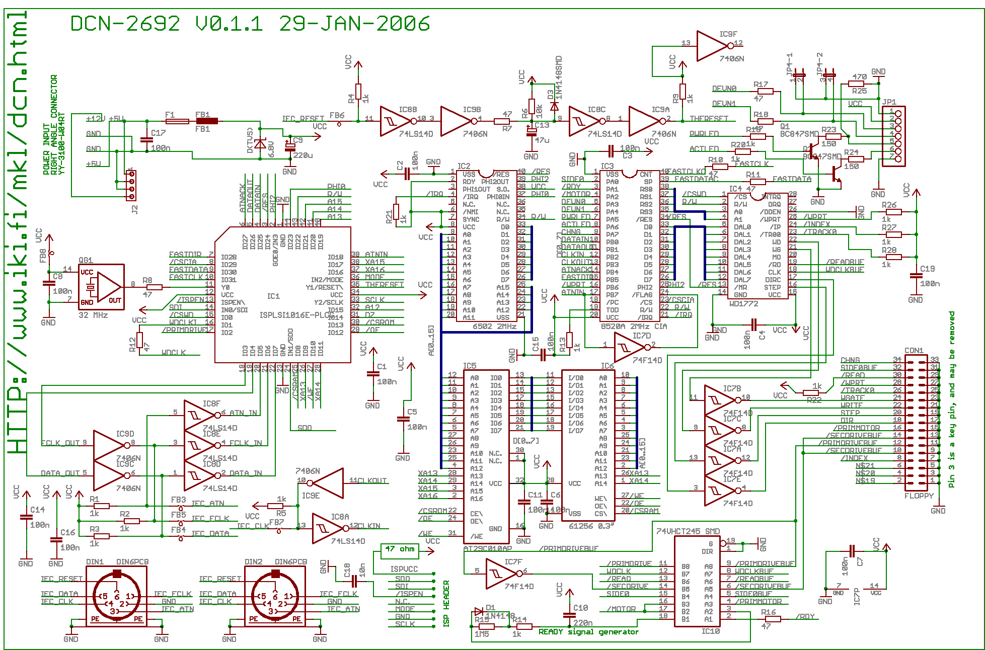
8520A vs 6526A CIA interface adapter IC:s
MOS/CSG CIA:s 8520 and 6526 are quite similar devices. 8520 does not have
the same "TOD"-clock that 6526 does have. 8520 seems to have more powerful
output at some pins, where as outputs from 6526 are capable of sinking
only 3.2 mA (min.) or sourcing 200 uA (min.) 1 mA (typ.)
That is the reason why there are some extra buffers
from the signals from CIA to Floppy-connector. The original C-1581 uses a 8520A.
The letter A in 8520A or 6526A means that the chips are rated for 2 MHz.
Links to more data here
VL1772
VL1772 should be compatible with WD1772
WD1772 vs WD1770 floppy controller IC:s
I have only used this controller with WD1772. WD1770 is quite compatible,
but it has a few differences. In the 1581 schematic it suggested that the
2 MHz PHI2 clock is connected to pin 19 of 8520A CIA, when WD1770 is used.
This pin is the input
for the counter, which is different between 6526 and 8520, so the combination
of 6526 and WD1770 might possibly not work? On DCN-2692, the pin 19 is
tied to VCC voltage level.
I remember reading somewhere that Commodore started using WD1772 instead of WD1770, when it was discovered
that some of the WD1770:s were faulty, and these could
corrupt data on disk.
ROM types
Atmel FLASH PEROM type AT29C010AP (128 KBytes) is used here. It is
reprogrammable without extra programming voltages, and it is possible
to reprogram it in-system. (Possibly also in this system in the future.)
The ROM socket should also accept other types of ROMs, including 28-pin
types, which should be inserted correctly to the 32-pin socket. It needs
to be at least 32 KiloBytes large to hold the original ROM content.
Ready signal
PC-drives differ from the standard. One thing missing is the drive ready
signal. Standard drives assert this signal, when the floppy disk is spinning at (almost?) full speed. It
should take about a half second after the motor has been turned on.
If it takes too long, the 1581 will give an error, saying
drive not ready.
This signal is emulated by R15, R14, D1, C10, and a buffer in IC10.
The component values were changed between V0.0.4 and V0.1.0.
74VHCT245 used in some boards has 8mA drive, maybe not enough for two drives like 74ls245 (24mA sink/15mA source). (Also, no support coded for 2 drives anyway) 74ls245 has 0.2V min. hysteresis, while nxp 74vhct "All inputs" (IO's too?) "have Schmitt-trigger action" but no specified hysteresis. Also, 74ls245 has schottky diodes which would "terminate" overshooting signals (reflections). A 74F245 is not recommended, it can e.g. output oscillations from "ready-signal simulator circuit". The latter can have RC time constant from C/R
220uF/1.5K 100uF/3.3K 47uF/6.8K or 33uF/10K
There is a slim chance that a PC floppy drive has the Ready signal
somewhere on its circuit board.
Compatibility with Commodore 1581
This should be compatible. But I had trouble with cbm4win and my PC;
copying files to dcn-2692 caused the transfer to hang many times, but
this could have happened because of possibly slowish transistors I used
in the XA1541 adapter.
There are known differences, but I don't know whether these do cause
any compatibility issues:
The lowest 16 KBytes of SRAM is visible at the lowest 16 KByte range of
the 6502. The C1581 has 8 KBytes of RAM, and it is (IIRC) mirrored to
6502 address space 2000..3FFF.
The ready signal from the floppy drive is simulated so, that the CIA
senses the simulated "ready" going low (=active) about 0.5
seconds after the CIA drives the "motor" signal of the floppy drive low
(=active.)
Please note that I haven't tested the board with the C128 fast burst
transfer mode.
CPLD files and download cable schematic
Some of the logic (e.g. glue logic, etc.) is placed on a programmable
logic chip. CPLD stands for Complex Programmable Logic Device. Such an
IC can be user programmed and
be used instead of standard TTL/CMOS logic ICs, such as 74LS00 etc.
The type used with this board is Lattice Semiconductor ispLSI1016E-80LJ
(where J stands for PLCC package.) It should also be possible to use the
ispLSI1016 or ispLSI1016EA version, and any speed grade will be fast enough.
But it is needed to recompile the ABEL source for each version of the CPLD.
dcn2.abl ABEL sourcefile for the CPLD, date
20-May-2003
dcn2.jed bitfile for ispLSI1016E-80LJ download
jedec file for isplsi1016 plc44 made from same source as ispLSI1016E jedec
No future versions of cpld code planned - no support for 2nd drive or ROM paging
Lattice Semiconductor website
Download software that programs the PLD with a .jed bit-file (windblows
pc and perhaps also x86 Linux). They might ask for registration,
etc.
Simplified isp download cable without "components".
ISP header  LPT port DB25
|1 VCC | -> 15. (VCC sense)
|2 SDO | -> 10.
|3 SDI | <- 2.
|4 _iE | <- 5.
|5 N.C.|
|6 MODE| <- 4.
|7 GND | <->GND Pins 18 through 25
|8 SCLK| <- 3.
\______/
         ,-< 8  Sense loop back
         `-> 12
ispLSI download cable. This "schematic" doesn't have the series resistors and caps.
(No guarantee there's no errors, but it should be almost ok.)
You could use small value (47-100 ohm) series resistors for signals
and a decoupling capacitor (1-1000 nF) between VCC and GND.
__
_iE is short for ispEN
ISP header ______74HC367______ LPT port
|1 VCC | -> |(16) VCC | -> 15. (VCC sense)
|2 SDO | -> |(2) 1A1 - 1Y1 (3) | -> 10.
|3 SDI | <- |(5) 1Y2 - 1A2 (4) | <- 2.
|4 _iE | <- |(11) 2Y1 - 2A1 (12)| <--5.
|5 N.C.| | /1OE(1)| <-� (read: "connect this to LPT pin 5. too")
|6 MODE| <- |(9) 1Y4 - 1A4 (10)| <- 4.
|7 GND | <->|(8) GND | <->GND Pins 18 through 25
|8 SCLK| <- |(7) 1Y3 - 1A3 (6) | <- 3.
\______/ | |(14) 2A2 tie this unused input either low or high
| /2OE (15)| <->GND Pins 18 through 25
\___________________/
,-< 8 Sense loop back
`-> 12
Images from from isp download cable pdf (june 2000.)
header pins
schematic
Image from Lattice isp manual pdf(1996)
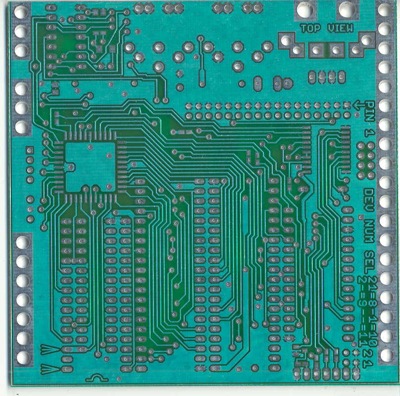
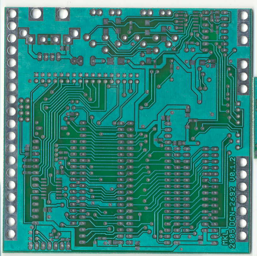
Versions, schematics, layouts, photos, etc.
Version history
5 pcs of v0.2.0
10 pcs of V0.1.5 were made.
PCB Version 0.1.2: I had one pce factory made.
PCB Version 0.1.1: I haven't built this one. 100 x 100 mm board
size. PCB masks are in a single A4 size Postscript sheet. All holes
are 0.3 mm "drill guide holes", for hand drilling aide. The
schematic is in PNG format.
PCB version 0.1.0: 6 pcs of these came from a PCB factory.
A number of small changes since 0.0.4, for example 7406 IC is
now in DIL-14 package instead of SMD SOIC-14.
PCB version 0.0.4: This is the same as version 0.0.2 with updated
documents, eg. component values were added to the schematic.
PCB version 0.0.2: 11 pcs of this board were made at a PCB factory.
PCB version 0.0.1: First prototype, PCB etched at home.
About the components, Some notes
Version 0.0.2 is the same as 0.0.4, but the schematic diagram v0.0.4 is
updated. (It has component values.)
Please note that the BOM (bill of materials) files are not fully
exact or complete, that means the raw BOMs are not perfect shopping
lists.
The 47 ohm series resistors R10, R11, R17 and R18 were added there to protect
the CIA I/O pins from "over-current", but maybe could be omitted and
replaced with solder blobs.
The 47 ohm series resistor R8 and R12 are like source termination
resistors for the clock lines 32MHz and WDCLK. The value 47 ohm
is only a guess, actually good value would depend on the impedance
of a transmission line. C1581 also used ferrite beads in series for
these lines.
The power supply line ferrite bead (FB1, or L1 in some schematic
versions) should be of a higher current type than the type used
for small signals. If the ferrite gets saturated, it doesn't do
a good job in suppressing RF noise leaving or entering the voltage
supply connector. I have not actually made any EMI measurement
if this component here has any significance, or could it be replace
with something better or a wire link.
The power supply connector does not appear in the genereated BOMs in the
table. The "correct" type of 5.25"-drive/3.5"-HDD power input connector
is the one which is normally mounted the other, and not the other
side of the CDROM/3.5"-HDD/5.25"-floppydrive PCB.
The 4-pin smaller (2.50 mm pitch) power connect on the board is not
actually the same type that appears in the BOMs, but instead the type
used with 3.5" floppy disk drives.
An 47 ohm SMD resistor does not appear in the generated BOMs. Its job
is to limit the current in case there happens a short circuit to ground
when plugging in the CPLD programming cable. (This sometimes happens
with my self built programming cable, which has the other row of two row
flat cable connector connected to ground.)
The ispLSI programming connector header does not appear in the generated
BOMs except for V0.0.4. It is an 8-pin 0.1" pitch header, where one
no-connection pin can be removed, and actually should be removed,
starting from V0.1.1.
74VHCT245 was used here because its CMOS sensitivity allows use of small
value (220 nF) capacitor with a larger value resistor (1.5 Mohm) in
the Ready signal simulator circuit, but 74ls245 should have more drive current (and using larger cap and smaller resistor.)
Connector "Floppy" is an 34-pin IDC connector / dual row pin header,
where one pin (number 3) should be removed.
Bugs
The series base resistor values (1 kohm) for BC847 npn transistor values are
too small, because the 6526 type CIA typically sources only about one
milliampere. So resistor values of R19 and R20 should be increased to 8.2 kohms.
(26-march-2006) Also, these led drivers could be replaced with prebiased transistor (bcr133) or fets (2n7002)
According to datasheets, the 6502 requires voltage swing to full VCC (=5 volts)
at the clock input. But the ispLSI1016 only outputs about 4 volts at high
logic level. The controller seems to work despite of that. 2.2kohm resistor pull-up would do "something" to that.
Diode D2 in ready-signal-generator-circuit is superfluous and may be omitted.
There is a bug in the factory made v0.1.0 PCB:s It is a short missing VCC
trace between two pull-up resistors R26 and R27 on the underside, near
IC4(WD1772). The missing trace is added in these V010 postscript files below
(V0.1.0a in table), so it is a slight bit different from the factory made
ones in this good way.
Copy paste from BOM-file for v0.1.0: IC7 (74LS14D) could be replaced
with 74F14D, which have "stronger" outputs, which might be needed when
driving the signals to two drives on the same cable, instead of only one
drive on the cable. Usually each drive has 1 kohm pull up on the
signals. For a logic TTL-low, an input must sense "at most" 0.8 volts, (but for schmitt trigger input better would be lower than 0.8 volts),
and that implies also a current. If there are two drives on a cable,
the combined pull up resistance would be 0.5 kohm, which requires more
current sinking capability from the signal driver.
Usage
You may use these documents to build a board, but you will responsible that
you can build it safely, and not burn your hand with a soldering iron and
not become blind with dangerous PCB manufacturing chemicals etc. And of
course there is no warranty that it will work, or work reliably.
Table
BUGS appearing in these document files:
see the "Bugs" paragraph above.
A few pictures
One 0.1.0 board
A board placed in a case from an ocn118 drive
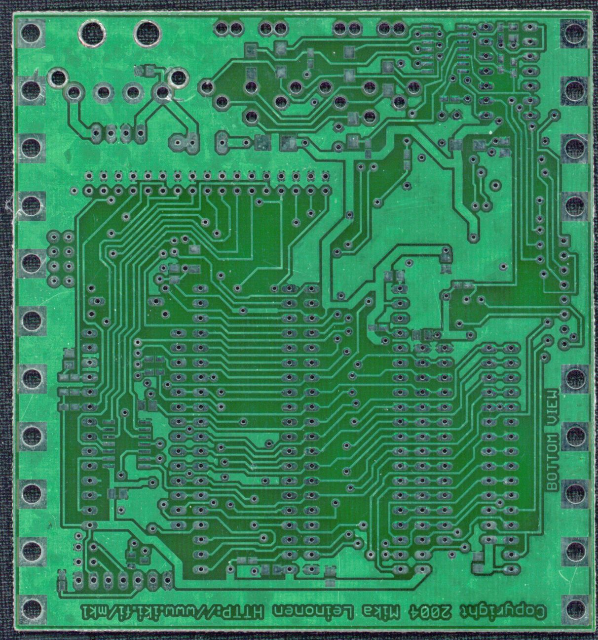
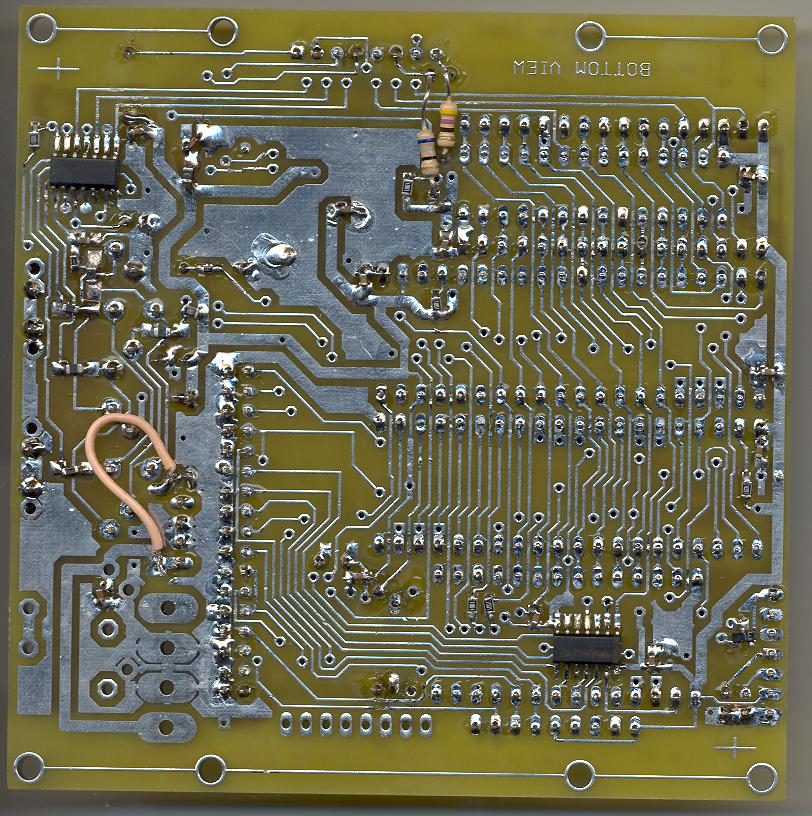
Underside view